PIC Analog to Digital Converter tutorial
A/D Theoretical background
The role of the ANALOG-TO-DIGITAL CONVERTER (A/D) is to convert analog voltage values to digital values. Lets explore the principle of operation of the A/D converter:
The ATD CONVERTER converts analog voltage to binary numbers. These binary numbers can be in different length - 2, 4, 8, 10-bit. The more bits the binary number has, the higher the resolution of the - A/D.
For example: Suppose that the voltage that supplied to the A/D converter varies from 0 to 5 volt, and the A/D converter converts the input voltage to a binary number of two-bits.
With two bits, we can ONLY display 4 different options:
| 00 | 01 | 10 | 11 |
That is, we can show the changes from 0 to 5 volt with 4 numbers, or more precisely four levels.
You can see the 4 levels in the following illustration:
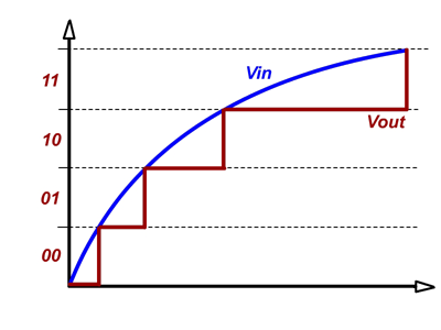
BLUE line describes the changes in the input voltage of the ANALOG-TO-DIGITAL CONVERTER (A/D) of the microcontroller.
RED line represents the digital levels at the output of the ANALOG-TO-DIGITAL CONVERTER (A/D) of the microcontroller.
We can see that the red signal far from being ideal, i.e. not close enough to the original analog input voltage values. Thus, we can say that A/D with the binary number of two-bits has a low resolution and there is a large gap between the real value of the analog input voltage and the values represented by the A/D.
Now, suppose that the voltage that supplied to the A/D converter is still varies from 0 to 5 volt, however, the A/D converter converts the input voltage to a binary number of three-bits.
With three bits we can get 8 different options:
| 000 | 001 | 010 | 011 | 100 | 101 | 110 | 111 |
That is, we can show the changes from 0 to 5 volt with 8 numbers, or more precisely 8 levels.
You can see the eight levels in the following illustration:
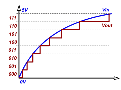
Now we can see that the RED line represents the original signal better than the previous RED line. The gap between the analog signal and the digital signal smaller compared to the previous graph. Based on the "good" results that we received, we can say that current A/D converter has a high-resolution compare to previous case.
Therefore we can say that the ANALOG TO DIGITAL CONVERTER (A/D) of the microcontroller with a larger amount of bits has a higher resolution and better accuracy when converting from analog signal to digital signal.
There is another fact to mention about the resolution of the A/D converter. Since the converter converts the signals, it takes a certain time. The conversion time of the low resolution A/D takes less time than the conversion time of the high resolution A/D.
When you are planning special systems, you have to take into account this fact. If you are planning to build accurate and fast systems, you have to consider carefully which convert to choose: if you select A-to-D with high resolution system will not be as fast; but if you select an A-to-D with high-speed response you will loose the resolution of the system.
How to convert analog values to digital values:
If we decide to work with an analog to digital converter (A/D) with three-bit length, we obtain eight different binary numbers which represent different voltage levels. For example:
| Voltage levels [V] | Binary representation |
| 0-0.62 | 000 |
| 0.621-1.25 | 001 |
| 1.251-1.87 | 010 |
| 1.871-2.5 | 011 |
| 2.51-3.12 | 100 |
| 3.121-3.75 | 101 |
| 3.751-4.37 | 110 |
| 4.371-5.00 | 111 |
In this example, the analog voltage values from 0v to 0.62v have a binary representation of 000; the analog voltage values from 0.621v to 1.25v have a binary representation of 001 so on.
The ADCON module located within the PIC microcontroller has a resolution of ten-bit length. Therefore, the converter can divide the analog input voltage between 0v and 5v to 2^ 10 levels, which are 1024 levels. We can say that the resolution of this component is very high.
How do we know what is the binary value/representation of the analog input voltage?
We can use the triangle method to calculate/find the binary representation of an analog input voltage. For example, lets calculate/find the binary value representation on the analog input voltage of 3.65 volt:
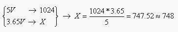
The analog input voltage of 3.65v will be represented by decimal number 748 or by binary number 1011101100.Using similar way we can find a binary representation for any desired level of the analog input voltage.
The A/D module has four 8 bit registers. These registers are:
- ADCON0 - A/D Control Register 0; determines the behavior of the A/D
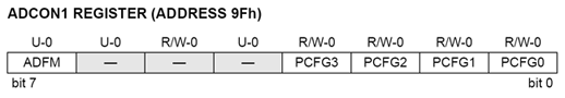
- ADCON1 - A/D Control Register 1; determines the configuration of the PORTA and PORTE and how the result of conversion of A/D will be store
- ADRESH - A/D Result High Register
- ADRESL - A/D Result Low Register
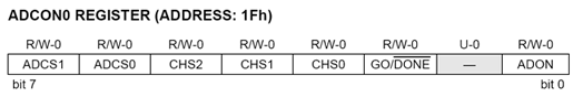
The size of this register is one byte (8 bits). Each bit has an important role in the definition of the component. Here's a breakdown of the bits role:
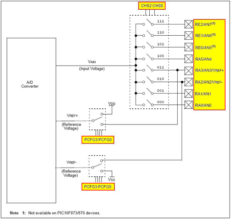
After we define the appropriate pins in the specific PORT to be analog inputs, we can sample the analog input voltage using one of the following channels:
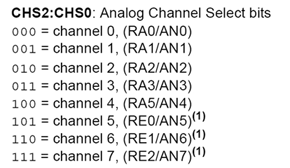
You can sample from PORTA each of the pins RA0 and RA5 except pin RA4 (used for other purposes) as well as of PORTE.
GO/DONE: A/D Conversion Status bit
If ADON = 1:
1 = A/D conversion in progress (setting this bit starts the A/D conversion)
0 = A/D conversion not in progress (this bit is automatically cleared by hardware when the A/D conversion is complete)
ADON: A/D On bit
1 = A/D converter module is operating
0 = A/D converter module is shut-off and consumes no operating current
The size of this register is one byte (8 bits). Each bit has an important role in the definition of the component. Here's a breakdown of the bits role:
ADFM: A/D Result Format Select bit
1 = Right justified. 6 Most Significant bits of ADRESH are read as 0.
0 = Left justified. 6 Least Significant bits of ADRESL are read as 0.
As we said, the A/D converter has a resolution of ten bits, i.e., the result of the conversion can not be stored in one register of eight bits.
.
Therefore, the result is stored in two registers: ADRESL and ADRESH. The size of each register is 8 bits long, so that we have 16 (2*8) bits all together.
We can store the result of the conversion which is 10 bits long using the two registers ADRESL and ADRESH in the following 2 ways:
- alignment to the left
- alignment to the right
Alignment to the left the eight MSB bits are stored in the ADRESH, and the two LSB bits are stored in ADRESL. In this case, the remaining six bits appear as - "0".
| Left Justified | |||||||||||||||
| X | X | X | X | X | X | X | X | X | X | 0 | 0 | 0 | 0 | 0 | 0 |
| ADRESH | ADRESL |
Alignment to the right the eight LSB bits are stored in ADRESL, and two MSB bits are stored in the ADRESH. In this case six highest bits appear as - "0".
| Right Justified | |||||||||||||||
| 0 | 0 | 0 | 0 | 0 | 0 | X | X | X | X | X | X | X | X | X | X |
| ADRESH | ADRESL |
PCFG3:PCFG0: A/D Port Configuration Control bits:
With these bits we can control the pins of PORTA or PORTE. We can decide an analog (A) or digital (D) mode.
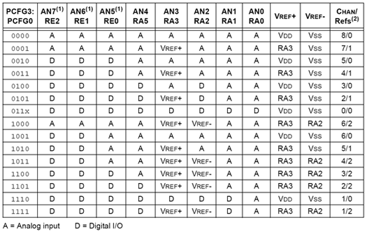
If we want to work with the PORTA and PORTE as analog ports, then we select the option PCFG3: PCFG0 = 0000; If we want to work with ports as digital, then we select the option PCFG3: PCFG0 = 011x.
In general, after the specified desired behavior of the A/D converter unit and before we start the conversion operation, we have to set up channel through which the analog information will be received using TRIS command. To begin making the conversion, we have to set the GO/DONE =1. This is done by using the command ADGO = 1. When the conversion ends, the result will be loaded into 2 registers ADRESH: ADRESL. Status bit GO/DONE (the register ADCON0) will be set to zero and the ADIF flag is set.
Analog to Digital BLOCK DIAGRAM
To summarize, the following steps should be followed for doing an A/D Conversion:
- Configure the A/D module:
- Configure analog pins/voltage reference and digital I/O (ADCON1)
- Select A/D input channel (ADCON0)
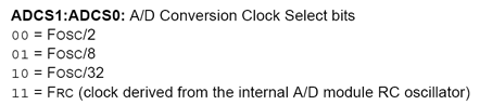
- Select A/D conversion clock (ADCON0)
- Turn on A/D module (ADCON0)
- Configure A/D interrupt (if desired):
- Clear ADIF bit
- Set ADIE bit
- Set PEIE bit
- Set GIE bit
- Wait the required acquisition time.
- Start conversion:
- Set GO/DONE bit (ADCON0)
- Wait for A/D conversion to complete, by either:
- Polling for the GO/DONE bit to be cleared(with interrupts enabled); OR
- Waiting for the A/D interrupt
- Read A/D result register pair (ADRESH:ADRESL), clear bit ADIF if required.
- For the next conversion, go to step 1 or step 2, as required.