PIC16F87XA memory organization tutorial
PIC microcontroller is very convenient choice to get started with a microcontroller projects.
In this PIC16F87XA memory organization tutorial we will study:
- 3 types of memories - Program Memory, Data Memory, and Data EEPROM
- Important registers - STATUS register, TRIS register, and PORT register
- direct and indirect addressing
- how to write to Data EEPROM
- how to read from Data EEPROM
Memory of the PIC16F877 divided into 3 types of memories:
- Program Memory - A memory that contains the program(which we had written), after we've burned it. As a reminder, Program Counter executes commands stored in the program memory, one after the other.
- Data Memory This is RAM memory type, which contains a special registers like SFR (Special Faction Register) and GPR (General Purpose Register). The variables that we store in the Data Memory during the program are deleted after we turn of the micro.
- Data EEPROM (Electrically Erasable Programmable Read-Only Memory) - A memory that allows storing the variables as a result of burning the written program.
These two memories have separated data buses, which makes the access to each one of them very easy.
Each one of them has a different role. Program Memory and Data Memory two memories that are needed to build a program, and Data EEPROM is used to save data after the microcontroller is turn off.
Program Memory and Data EEPROM they are non-volatile memories, which store the information even after the power is turn off. These memories called Flash Or EEPROM. In contrast, Data Memory does not save the information because it needs power in order to maintain the information stored in the chip.
PIC16F87XA Program Memory
The PIC16F87XA devices have a 13-bit program counter capable of addressing an 8K word x 14 bit program memory space. This memory is used to store the program after we burn it to the microcontroller. The PIC16F876A/877A devices have 8K words x 14 bits of Flash program memory that can be electrically erased and reprogrammed. Each time we burn program into the micro, we erase an old program and write a new one.
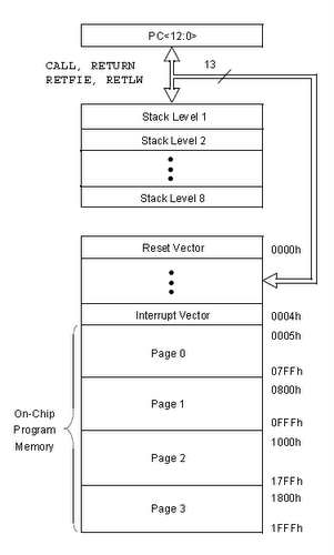
PIC16F876A/877A program memory map and stack
Program Counter (PC) keeps track of the program execution by holding the address of the current instruction. It is automatically incremented to the next instruction during the current instruction execution.
The PIC16F87XA family has an 8-level deep x 13-bit wide hardware stack. The stack space is not part of either program or data space and the stack pointer is not readable or writable. In the PIC microcontrollers, this is a special block of RAM memory used only for this purpose.
The CALL instruction is used to jump to a subroutine, which must be terminated with the RETURN instruction. CALL has the address of the first instruction in the subroutine as its operand. When the CALL instruction is executed, the destination address is copied to the PC. The PC is PUSHed onto the stack when a CALL instruction is executed, or an interrupt causes a branch. The stack is POPed in the event of a RETURN, RETLW or a RETFIE instruction execution.
The stack operates as a circular buffer. This means that after the stack has been PUSHed eight times, the ninth push overwrites the value that was stored from the first push. The tenth push overwrites the second push (and so on).
Each time the main program execution starts at address 0000 - Reset Vector. The address 0004 is reserved for the interrupt service routine (ISR).
If we plan to use an interrupt, our program will begin after the Interrupt Vector; and if not we can start to write from the beginning of the Reset Vector.
Here is a code where we use interrupt:
ORG 0x000 ; processor reset vector

goto main ; go to beginning of main program

ORG 0x004 ; interrupt vector location

movwf w_temp ; save off current W register contents

movf STATUS,w ; move status register into W register

movwf status_temp ; save off contents of STATUS register

.

.

RETFIE


main
Some of the memory is divided into the pages that are designed for write/burn the program into them; the remaining memory (Stack, Interrupt Vector, and Reset Vector) is hardware registers.
Attention!
Program Memory is divided into the pages, where the program is stored. Data Memory is divided into the banks. The banks are located inside the RAM, where the special registers and the data located.
PIC16F87XA Data Memory Organization
The data memory is partitioned into multiple banks which contain the General Purpose Registers and the Special Function Registers. Number of banks may vary depending on the microcontroller; for example, micro PIC16F84 has only two banks.
Each bank extends up to 7Fh (128 bytes). The lower locations of each bank are reserved for the Special Function Registers. Above the Special Function Registers are General Purpose Registers, implemented as static RAM. While program is being executed, it is working with the particular bank. The default bank is BANK0.
To access a register that is located in another bank, one should access it inside the program. There are special registers which can be accessed from any bank, such as STATUS register.
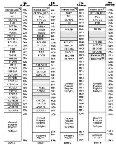
PIC16F876A/877A register file map
In order to start programming and build automated system, there is no need to study all the registers of the memory map, but only a few most important ones:
- STATUS register changes/moves from/between the banks
- PORT registers assigns logic values (0/1) to the ports
- TRIS registers - data direction register (input/output)
You can learn about other registers at a later stage or as needed.
STATUS register
In most cases, this register is used to switch between the banks (Register Bank Select), but also has other capabilities.
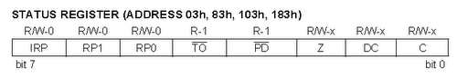
PIC STATUS register
With the help of three left bits (IRP, RP1, and RP0) one can control the transition between the banks:
- IRP - Register Bank Select bit, used for indirect addressing method.
- RP1:RP0: - Register Bank Select bits, used for direct addressing method.
To distinguish between the two methods, at this point, the will use the definition of fundamental concepts. Later on, the two methods will be studied in detail.
When the IRP Equal to 0, the program will work with banks 0, 1.
When the IRP Equal to 1, the program will work with banks 2, 3.
The following table demonstrates, which of the Banks the program is working with, based on the selection of the RP0 and RP1 bits:
| RP1:RP0 | BANK |
| 00 | 0 |
| 01 | 1 |
| 10 | 2 |
| 11 | 3 |
An example of using STATUS register and Register Bank Select bit:
- bsf STATUS, 5 ; Change to Bank 1
- clrf TRISB ; Set PORTB as output
- bcf STATUS, 5 ; Change to Bank 0
In the first line, we are in changing/setting the 5th bit, RP0, in the STATUS register to 1, and thus, base on the table we are switching/selecting Bank 1. After PortB was set as output in the second line, we switched back to Bank 0 by in changing/setting the 5th bit, RP0, in the STATUS register to 0, in the third line.
C: Carry/borrow bit (ADDWF, ADDLW,SUBLW,SUBWF instructions)
1 = A carry-out from the Most Significant bit of the result occurred
0 = No carry-out from the Most Significant bit of the result occurred
An example of using STATUS register and Carry/borrow bit:
- Movlw 200
- Addwf 100, 0
In this example, we are assigning value of 200 to the W (working) register. Then, we are adding the value of 100 and the W register together. The result is stored in W register and should be 300 (200+100).
However, the maximum value is 256, resulting in carry out. The C (bit 0) of the STATUS register becomes 1 (C = 1). Register W will contain the reminder: 44.
DC: Digit carry/borrow bit (ADDWF, ADDLW,SUBLW,SUBWF instructions)
(for borrow, the polarity is reversed)
1 = A carry-out from the 4th low order bit of the result occurred
0 = No carry-out from the 4th low order bit of the result
Z: Zero bit
1 = The result of an arithmetic or logic operation is zero
0 = The result of an arithmetic or logic operation is not zero
The bits 3 and 4 are used with WDT - Watchdog Timer.
PD: Power-down bit
1 = After power-up or by the CLRWDT instruction
0 = By execution of the SLEEP instruction
TO: Time-out bit
1 = After power-up, CLRWDT instruction or SLEEP instruction
0 = A WDT time-out occurred
PORT register
The role of the PORT register is to receive the information from an external source (e.g. sensor) or to send information to the external elements (e.g. LCD). The 28-pin devices have 3 I/O ports, while the 40/44-pin devices, like PIC16F877, have 5 I/O ports located in the BANK 0.
- PORTA is a 6-bit wide, bidirectional port. The corresponding data direction register is TRISA.
Setting a TRISA bit (= 1) will make the corresponding PORTA pin an input. Clearing a TRISA bit (= 0) will make the corresponding PORTA pin an output. - PORTB is an 8-bit wide, bidirectional port. The corresponding data direction register is TRISB.
Setting a TRISB bit (= 1) will make the corresponding PORTB pin an input. Clearing a TRISB bit (= 0) will make the corresponding PORTB pin an output. - PORTC is an 8-bit wide, bidirectional port. The corresponding data direction register is TRISC.
Setting a TRISC bit (= 1) will make the corresponding PORTC pin an input. Clearing a TRISC bit (= 0) will make the corresponding PORTC pin an output. - PORTD is an 8-bit port with Schmitt Trigger input buffers. Each pin is individually configurable as an input or output.
- PORTE has three pins (RE0/RD/AN5, RE1/WR/AN6 and RE2/CS/AN7) which are individually configurable as inputs or outputs. These pins have Schmitt Trigger input buffers.
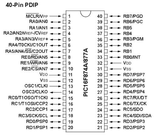
Pin diagram of PIC16F877A
We can control each port by using an assigned address of specific port, but there is much easier way to control the port. We are allowed to use the names of the ports without considering their addresses.
For example:
# define SWITCH PORTA, 0
We define a variable named SWITCH, which received a value of bit number 0 of the PORTA. Usually we define the ports at the beginning of the program, and then we use only the given names.
TRIS register
The TRIS register is data direction register which defines if the specific bit or whole port will be an input or an output. Each PORT has its own TRIS register. Here's a map of the locations:
| BANK0 | BANK1 |
| PORTA | TRISA |
| PORTB | TRISB |
| PORTC | TRISC |
| PORTD | TRISD |
| PORTE | TRISE |
The default mode of each TRIS is input. If you want to set a specific port as exit you must change the state of the TRIS to 0.
Keep in mind: to change a specific port to an output, one should first move to the BANK1, make the change, and then return to BANK0. The default state of the banks is BANK0.
The running program is working only with one bank at all time. If not set otherwise, then as stated, the default bank is BANK0. Part of the registers located inside BANK0, and some are not. When we need to access a register that is not located inside BANK0, we are required to switch between the banks.
For example, the access to PORT registers is done inside BANK0. However, to change port from an input to an output and vice versa, we need to access TRIS register that is located inside BANK1. From the moment we moved to the BANK1, the program will always work with BANK1; at this time, to access registers inside BANK0, we will have to return to the situation in which our program will work with BANK0.
CLICK HERE to access PIC16F877A data sheet for more in formation on PIC memory organization
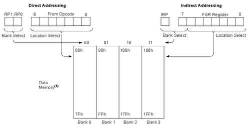
Direct and Indirect addressing
Direct Addressing: Using this method we are accessing the registers directly by detecting location inside Data Memory from Opcode and by selecting the bank using bits RP1 and RP0 of the STATUS register.
Indirect Addressing: To implement indirect addressing, a File Select Register (FSR) and indirect register (INDF) are used. In addition, when using this method we choose bank using bit IRP of the STATUS register. Indirect addressing treated like a stack pointer, allowing much more efficient work with a number of variables. INDF register is not an actual register (it is a virtual register that is not found in any bank).
Dont be confused! There is SFR (Special Function Register) - special registers of RAM, and there is FSR (File Select Register).
The following figure shows the two addressing methods:
Pin diagram of PIC16F877A
To the left you can see the direct addressing method, where the bank selection is made by RP bits and the referencing is made directly from memory Opcode by using the variable name.
To the right you can see the indirect addressing method, where the bank selection is made by IRP bit and accessing the variable by pointer FSR.
Lets explore the differences between the 2 methods:
We want to assign number 5 to the variable TEMP located at address 0X030. In the first row of each example, we will define the variable TEMP at the address 0X030.
Example of direct addressing:
- TEMP Equ 0x030
- Movlw 5
- Movwf TEMP
It's easy to understand, that direct addressing method means working directly with the variables. In the second line we put the number 5 into the working register W, and in the line 3, the content of the W passes to the TEMP variable .
Example of indirect addressing:
- TEMP Equ 0x030
- Movlw 0x030
- Movwf FSR
- Movlw 5
- Movwf INDF
In the second line, we put a value into the W register. In the third line, the value passes to the FSR register, and from this moment FSR points to the address of the TEMP variable. In the fourth line, the number 5 passes to the W register, and in the fifth line, we move the contents of W register (which is 5) to the INDF. In fact INDF performs the following: it takes the number 5 and puts it in the address indicated by FSR register.
PIC16F87XA Data EEPROM
The data EEPROM and Flash program memory is readable and writable during normal operation (over the full VDD range). This memory is not directly mapped in the register file space. Instead, it is indirectly addressed through the Special Function Registers.
There are six SFRs used to read and write to this memory:
- EECON1
- EECON2
- EEDATA
- EEDATH
- EEADR
- EEADRH
When interfacing to the data memory block, EEDATA holds the 8-bit data for read/write and EEADR holds the address of the EEPROM location being accessed. These devices have 128 or 256 bytes of data EEPROM (depending on the device), with an address range from 00h to FFh. On devices with 128 bytes, addresses from 80h to FFh are unimplemented.
A few important points about Data EEPROM memory:
- It lets you save data DURING programming
- The data is saved during the burning process
- You can read the data memory during the programming and use it
- The use is made possible with the help of SFR
At this point there is no need to learn how to use this memory with special registers, because there are functions (writing and reading) that are ready.
Write to DATA EEPROM
To write to an EEPROM data location, the user must first write the address to the EEADR register and the data to the EEDATA register. Then the user must follow a specific write sequence to initiate the write for each byte.
BSF STATUS, RP1 ;
BSF STATUS, RP0 ; Bank 3
BTFSC EECON1, WR ;Wait for write
GOTO $-1 ;to complete
BCF STATUS, RP0 ;Bank 2
MOVF DATA_EE_ADDR, W ;Data Memory
MOVWF EEADR ;Address to write
MOVF DATA_EE_DATA, W ;Data Memory Value
MOVWF EEDATA ;to write
BSF STATUS, RP0 ;Bank 3
BCF EECON1, EEPGD ;Point to DATA memory
BSF EECON1, WREN ;Enable writes
BCF INTCON, GIE ;Disable INTs.
MOVLW 55h ;
MOVWF EECON2 ;Write 55h
MOVLW AAh ;
MOVWF EECON2 ;Write AAh
BSF EECON1, WR ;Set WR bit to begin write
BSF INTCON, GIE ;Enable INTs
BCF EECON1, WREN ;Disable writes
Read DATA EEPROM
To read a data memory location, the user must write the address to the EEADR register, clear the EEPGD control bit (EECON1<7>) and then set control bit RD (EECON1<0>). The data is available in the very next cycle in the EEDATA register; therefore, it can be read in the next instruction. EEDATA will hold this value until another read or until it is written to by the user (during a write operation).
BSF STATUS, RP1 ;
BCF STATUS, RP0 ; Bank 2
MOVF DATA_EE_ADDR, W ; Data Memory
MOVWF EEADR ; Address to read
BSF STATUS, RP0 ; Bank 3
BCF EECON1, EEPGD ; Point to Data memory
BSF EECON1, RD ; EE Read
BCF STATUS, RP0 ; Bank 2
MOVF EEDATA, W ; W = EEDATA
Both of these functions are provided by the manufacturer. There is a required sequence in order to write/read to/from the memory; that process can be performed independently, but it is better to use ready functions of Microchip.